


Detailed Explanation of Core Chips and Interface Technology for LED Displays: Key Principles & Maintenance Guide
The normal operation of LED displays relies on the coordinated work of three types of LED display core chipsand key interfaces such as the HUB75 interface. This article will systematically analyze the HUB75 interface pin definition, functional characteristics, LED chip pin definition, and LED display signal transmission logicof the three core chips, helping engineers, maintenance personnel, and industry enthusiasts deeply understand the hardware working principle of LED displays.
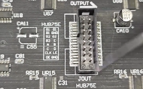
I. HUB75 Interface: The Core Hub of LED Display Signal Transmission
The HUB75 interface is the most widely used signal interface for indoor and outdoor LED displays, featuring 16 pins with clearly defined functions, which is a key channel for stable signal input of LED displays.
• The first 4 pins are the first group of color signals (RGB+GND), responsible for transmitting basic red, green, and blue color signals to ensure accurate color reproduction of the LED display.
• The next 4 pins are the second group of color signals (R2, G2, B2+GND), further expanding the color transmission dimension and improving the color depth of the display.
• The middle 4 pins (A, B, C, D) are LED display row signals, specifically controlling the on/off state of the row control chips.
• Among the last 4 pins, CRK, ARE, and OE are public signals mainly acting on the color column chips, while GND is the negative electrode to ensure the stable
operation of the LED display circuit.
II. Three Types of LED Display Core Chips: Functions, Pins, and Signal Transmission Logic
The core chips of LED displays are divided into 245 signal amplification chips, LED color column chips, and LED row control chips, with clear divisions of labor to jointly support the high-definition and stable display of the screen.
(1) 245 Chip: The “Signal Amplification Bridge” for LED Displays
The 245 chip (e.g., DP245) has a 20-pin structure, and its core function is LED signal amplification to solve the problem of signal attenuation during long-distance transmission.
• Pin definition: Pins B0-B7 on the right are 8 input pins, and pins A0-A7 on the left are 8 output pins, realizing one-way signal transmission and amplification.
• Signal transmission principle: Color signals from the HUB75 interface are input to the input pins of the 245 chip, amplified internally to enhance signal strength, and then transmitted to the color column chips from the output pins to ensure clear signal reception.
(2) Color Column Chip: The “Color Control Core” of LED Displays
The LED color column chip (common models: 595, DP32020) mostly has a 24-pin structure, which is the key component for controlling the color display of LED screens and the most numerous chip in the display module.
• Pin definition: Pins OUT0-OUT15 at the bottom are 16 output pins connected to LED lamp beads, while the 8 pins at the top include GND (negative electrode), SDR (signal input), and public signal pins such as CRK and ARE.
• Signal transmission process: It receives amplified color signals from the 245 chip, processes them internally, transmits them to the corresponding LED lamp beads through the output pins to realize color lighting, and simultaneously cascades the signals to subsequent color column chips via the SDO pin to expand the display area.
• Resistor matching function: The 23rd pin is connected to an external resistor, and different resistance values correspond to red, green, and blue colors to control the brightness of each color; resistor damage or mismatched resistance values will cause abnormal phenomena such as dark screens or color distortion of the LED display.
(3) Row Control Chip: The “Row Driving Switch” of LED Displays
The LED row control chip is responsible for driving the row scanning of the display, with one chip capable of controlling 8 rows of LED lamp beads, divided into old and new models to adapt to different display module designs.
• Old models (e.g., RCN2012, 74H138): The power supply pin is VDD (5V), and pins A2, A1, A0 are signal input pins that receive row signals amplified by the 245 chip to control the on/off of the corresponding rows.
• New models (e.g., 5958, DP32020): The pin definition is similar to that of color column chips, with pin 2 as the signal input, pin 10 as the serial signal output, pins 3 and 4 as public signals, and pins OUT0-OUT7 as 8 output pins to drive row lamp beads.
• Signal transmission characteristics: After receiving row signals, it controls the on/off of the corresponding 8 rows of lamp beads through the output pins, and the signals can be cascaded to subsequent row chips via the output pins to realize the scanning display of the entire screen.
III. Practical Guide: How to Query LED Chip Pin Definitions
Accurately querying LED chip pin definitions is a key step in LED display maintenance and debugging, which can be efficiently completed through professional tools.
• Recommended tool: Use the “Xinchacha” (Chip Checker) software, which is available for download from major app markets and supports querying pin definitions of most LED display chips.
• Step-by-step operation: Open the software and log in, enter the chip model (e.g., 245, DP32020, 74H138), click the search button, and view the corresponding data sheet to obtain detailed pin functions and connection diagrams.
• Important notes: Some special chip models cannot be directly queried, but their pin definitions are consistent with general chips of the same type; there are differences in pin definitions between old and new row chips, which need to be distinguished by comparing with the data sheets of normal modules.
Detailed explanation of RGB color signal/row signal/public signal pin assignment of LED display HUB75 interface, analyzing signal transmission logic of 245 chip/color column chip to solve display fault diagnosis problems.